
Research at LMN
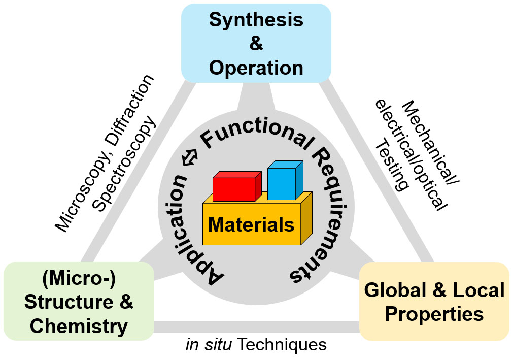
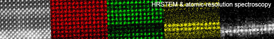
Our aim is to contribute to the development of novel materials with tailored properties as well as to the understanding and optimization of applied materials and devices. Therefore, we apply advanced and in situ light, electron and ion microscopy (TEM, SEM, FIB/SEM) in conjunction with complementary X-ray techniques in order to gain insight in the complex relationship between the material’s properties on the one hand and its (local) microstructure, crystal structure and chemistry on the other (figure on the right).
Moreover, we utilize and develop cryo and in situ EM techniques to understand materials under application-relevant conditions as well as to measure material properties down to the nm-scale. In addition to such materials characterization, which we offer to other university groups and external collaborators, we conduct independent materials research (deposition, synthesis, testing, operation) on novel mesoporous metal foams, 2D semiconductors as well as energy materials and devices (batteries and fuel cells). Our research field are:
Scale-bridging characterization of complex and/or reactive/sensitive devices & sensors
- Structure formation, degradation/failure analyses of fuel cells, solar cells, batteries, gas/ion separators, optical sensors
- Cross-sectional/target preparation even of reactive devices / complex sensors for OM, SEM, TEM, etc
- Cryo-/inert-gas preparation, handing, characterization of highly reactive/sensitive samples
- in situ microscopy for clarification of structure-property relationships, structure formation, degradation/failure
Structure formation, phase transformations, ion transport
- Mechanical/electrical long-term stability, decomposition of ceramics, metals & composites
- Ion diffusion in battery materials & ceramics, impact of trace elements
- Impact of external stimuli like temperature, environment, pressure & load by in situ microscopy
- Impact of strain on electron and ion transport in complex composite materials
Defects and interfaces
- Structure, chemistry and properties of interfaces in solids
- Evolution of interfaces in devices during operation
- Impact of defects on electrical/mechanical properties
- Dislocations in graphene and other 2D materials
Development of advanced methods
- Inert-gas/cryo-transfer of sensitive materials for (in situ) EM & surface methods in STM, LEEM
- 4D-STEM/EELS of complex device/sensor cross-sections
- in situ EM: cooling/heating, mechanical/electrical testing, environmental EM
- Novel EM preparation techniques
Aktualisiert um 12:45 pm am December 30, 2019 von Benjamin Butz
