
TEM
Transmission Electron Microscope (TEM)
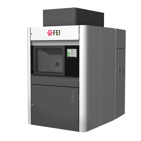
FEI Talos F200X
Our TEM is a FEI made model (Talos F200X) combined with an Energy Dispersive X-ray Analyser (EDX). A maximum accelerating voltage of 200 kV and high resolutions down to 0.25 nm are possible.
Appending informations:
Fieldemission cathode
•1,8e9 A/cm2
•Beam current: 1,5 pA
Resolution
•TEM-point resolution: 0,25 nm
•STEM HAADF: 0,16 nm
•EDX: 0,9nm
Diffraction
•Camera length: 12-5100mm
•Diffraction angle: +-12
Image and Video
•16 MP CMOS for images
•4k x 4k: 1fps
•512 x 512: 25fps
•Live-camera with 40 fps for searching manually
Substrateholder
•Single tilt for EDS
•Double tilt for EDS, rigid model
•tilt angle both axes +-30°
•For magnetic samples (z.B. DSS)
•optimized for highest resolution and EDS
•liquid Nitrogen cooled double tilt substrate holder for EDS
EDS
•Test time:
•t<10µs/point à 1e6 point/s
•105 spectra/s
Tomography
•Tilt angle +-75°
Miscellaneous
•Cool trap
•Piezodrive of sample position: 20pm step size
At our institute the F200X is used to obtain conventional electron micrographs of Carbon-based nano structures such as, carbon-nano-tubes(CNTs), carbon-nano-helices(CNHs), carbon-nano-fibres, tubular-graphitic-cones(TGCs), and thin film systems. Crystollographic information of the above stated materials is interpreted from the SAED patterns. Chemical compositional analysis of multi phase thin film systems is carried out using the EDS system.